
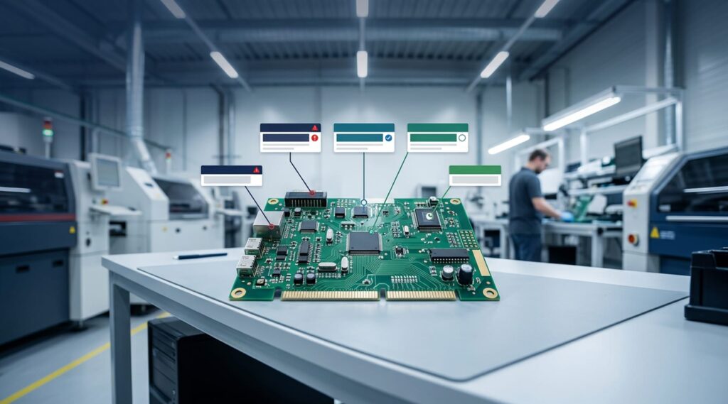
Bridging Layout Design and Manufacturing Reality
For engineering teams developing mission-critical hardware, releasing a complex PCB assembly to production is a high-stakes transition. A layout can simulate perfectly in CAD, adhere strictly to electrical rule checks, and still encounter severe bottlenecks once it reaches physical fabrication and surface mount assembly lines. When unvetted designs reach the manufacturing floor, the cost of correction multiplies exponentially in scrapped boards, stalled assembly lines, and extended verification delays.
A persistent industry myth suggests that thorough Design for Manufacturability (DFM) reviews introduce drag into hardware development cycles. In practice, bypassing early manufacturing analysis simply pushes latent layout deficiencies into prototype or full production runs. Addressing an engineering change order while pick-and-place machines sit idle consumes far more capital and calendar time than catching discrepancies in the design phase. A systematic pre-production DFM review surfaces physical constraints early, helping teams avoid unnecessary rework and supporting reliable, compliant builds. Below are five pre-production DFM checkpoints every hardware team should verify before committing to production tooling.
1. Component Availability and Lifecycle Status
Complex circuit boards frequently feature dense Bills of Materials (BOMs) comprising hundreds of unique line items. Designing around parts that are obsolete, nearing end-of-life, or encumbered by volatile lead times creates an immediate production hazard.
Production Risk: Sourcing disruptions discovered mid-build force emergency component substitutions. Swapping an IC after board layout completion can necessitate trace rerouting, pad modifications, and secondary compliance recertifications, effectively halting your production schedule.
Problem: An engineer selects a specialized power management IC showing nominal inventory at a catalog distributor during initial schematic capture. By the time layout sign-off occurs, the manufacturer issues an End-of-Life (EOL) notification, and factory lead times stretch to 48 weeks with zero authorized domestic inventory.
Fix: Replace the single-source IC with an active part that features pin-compatible alternate sources. Update the schematic and library symbols to accommodate a standardized footprint accepted by multiple manufacturers before finalizing the layout.
- Review Action: Screen every BOM item against real-time lifecycle databases to confirm Active status with multiple domestic distribution paths.
- Review Question: Does each mission-critical active device have at least one drop-in or pin-compatible alternate validated in the schematic?
2. Footprint Accuracy and Solder Land Geometry
CAD footprint libraries often rely on generic land patterns that fail to match the specific package variants delivered by component suppliers. Minute variations between manufacturer package drawings and CAD land patterns cause acute assembly defects during reflow.
Production Risk: Mismatched solder land dimensions lead to poor wetting, tombstoning of passive components, solder bridging on fine-pitch ICs, or inadequate solder fillets that fail structural inspection standards like IPC-A-610.
Problem: A high-speed microcontroller in a 0.4 mm pitch QFN package is assigned a footprint where the copper lands extend too far inward toward the exposed ground slug. During reflow solder deposition, surface tension pulls excess paste across the nominal gap, creating hidden solder bridges between peripheral input/output pins and the ground plane.
Fix: Recalculate land geometry using IPC-7351 guidelines. Shorten the inner pad extension to maintain a minimum 0.2 mm soldermask dam between signal pins and the central ground paddle, and segment the paste stencil aperture into a windowpane pattern to restrict paste volume.
- Review Action: Cross-check high-density footprints directly against the component manufacturer’s exact mechanical tolerance sheet rather than relying on unverified third-party libraries.
- Review Question: Have passive 0402 and 0201 packages been balanced in trace entry width to prevent thermal draw disparities that induce tombstoning?
3. Component Clearance and Physical Spacing
Packing high-reliability electronics into constrained form factors pushes layout clearances to the limit. However, automated surface-mount placement systems and automated optical inspection (AOI) equipment require dedicated clearance envelopes to operate without mechanical interference.
Production Risk: Parts placed too closely prevent pick-and-place nozzles from seating components accurately, shield shorter parts from reflow heat transfer, and create optical blind spots that impede automated inspection cameras, forcing costly manual assembly workarounds.
Problem: A tall electrolytic capacitor (12 mm height) is placed 0.6 mm away from a fine-pitch 0.5 mm SOIC sensor. During automated pick-and-place, the placement head vacuum nozzle collides with the pre-placed capacitor. Later in the process, the physical bulk of the capacitor blocks the line-of-sight lighting of the AOI camera, masking potential bridge defects on the sensor pins.
Fix: Reposition the capacitor to maintain a clearance of at least twice its height from adjacent low-profile surface-mount devices. Reorient the SOIC to provide an unobstructed optical sightline for automated camera inspection.
- Review Action: Run comprehensive 3D clearance checks inside your ECAD/MCAD environment, incorporating accurate component body height models (STEP files) rather than flat 2D courtyards.
- Review Question: Do all tall components adhere to assembly keep-out zones required by standard domestic manufacturing pick-and-place heads?
4. Thermal Constraints and Solder Balance
Unequal thermal mass across adjacent copper connections introduces severe soldering variability during production reflow and selective soldering processes.
Production Risk: Large internal ground and power planes act as massive heat sinks. If pads connect directly to solid planes without adequate thermal relief, heat wicks away from the joint during reflow, resulting in cold solder joints, incomplete wetting, and assembly fractures under field stress.
Problem: A multi-layer board features high-current inductive filters where one terminal is connected to an isolated surface trace and the other connects directly to an internal 2 oz ground copper pour without thermal relief. During convection reflow, the isolated pad heats rapidly while the ground pad fails to achieve liquidus temperature, causing tombstoning and an intermittent open connection.
Fix: Apply standardized 4-spoke thermal relief connections to all through-hole and surface-mount ground pads tying into inner plane copper. Ensure conductor width satisfies current density demands while providing adequate thermal isolation during soldering.
- Review Action: Audit the gerber copper layers to identify all plane ties on discrete passive pads and verify uniform thermal relief parameters across shared subcircuits.
- Review Question: Are large exposed thermal pads equipped with plated microvias designed to prevent solder evacuation into lower layers?
5. Test Access and Fixture Accessibility
A board that cannot be systematically tested cannot be reliably deployed. High-reliability manufacturing requires accessible electrical test points to validate assembly integrity via In-Circuit Testing (ICT) or Flying Probe testing before shipping.
Production Risk: Designs devoid of designated test points force reliance on functional testing alone. Functional tests cannot efficiently isolate individual component failures or pinpoint manufacturing process shifts, making fault diagnostic rework slow and labor-intensive.
Problem: A critical SPI communication bus running between a host processor and peripheral memory is routed entirely on inner board layers without break-out pads. When communication drops during initial board power-up, technicians cannot probe signals without manually scraping soldermask off traces under a microscope, risking copper damage.
Fix: Place dedicated 0.8 mm surface test pads on unmasked outer layers for every primary power rail, clock line, and peripheral communication bus. Standardize test point grid pitch to a minimum of 1.27 mm to accommodate reliable bed-of-nails fixture pins.
- Review Action: Generate a comprehensive test point report from layout software to confirm minimum percentage net coverage across all schematic signals.
- Review Question: Are test points kept clear of tall components by at least 2.5 mm to allow test fixture probe plate travel?
Pre-Production DFM Checklist
Before exporting CAM files and issuing production orders, perform this final verification pass with your team:
- BOM Lifecycle: Are all components actively manufactured, with domestic distributor stock confirmed and pin-compatible alternates identified?
- Footprint Verification: Have pad geometries, pin assignments, and courtyard dimensions been verified against vendor mechanical package drawings?
- SMT Clearances: Do tall components respect equipment head clearances and allow line-of-sight for Automated Optical Inspection (AOI)?
- Thermal Balance: Are surface-mount and through-hole connections to inner copper pours designed with proper thermal relief to prevent cold joints?
- Testability Coverage: Does the layout provide accessible, dedicated test pads on essential nets with sufficient spacing for mechanical probes?
Ensure Production Success with American Precision Electronics
Catching design conflicts on a computer screen costs a fraction of resolving assembly failures on the factory floor. While no engineering review can replace comprehensive verification, an early, disciplined DFM assessment significantly reduces technical risk and paves the way for clean, repeatable production runs.
American Precision Electronics operates from a modern 30,000-square-foot facility in Illinois, partnering with design teams to bring complex, high-reliability electronic assemblies to life. Involve APE early in your design cycle to review your layout, align with domestic manufacturing processes, and support your project with technical precision before you release to production.